PowerGraph: A Mobile Energy Measurement Framework for Mobile Devices
This page provides an overview of the actual hardware design of PowerGraph. PowerGraph itself consists of three boards, explained and depicted below. The overall costs for all the parts (including the Pi) sum up to around 70€.
Power board
This board accepts power through a USB cable and redistributes the power throughout the system. It connects directly to the Raspberry Pi's power input and the converter board. It also contains an a cinch plug that provides power to the smartphone or other devices.The voltage available at the cinch plug can be adjusted onboard. The output voltage range is approximately 0.6V-4.8V. For example, this allows to simulate different battery charge levels for the smartphone or provide compatibility for a wide range of devices. The power consumption of the device, connected at the cinch plug, is measured and the result if forwarded to the converter board.
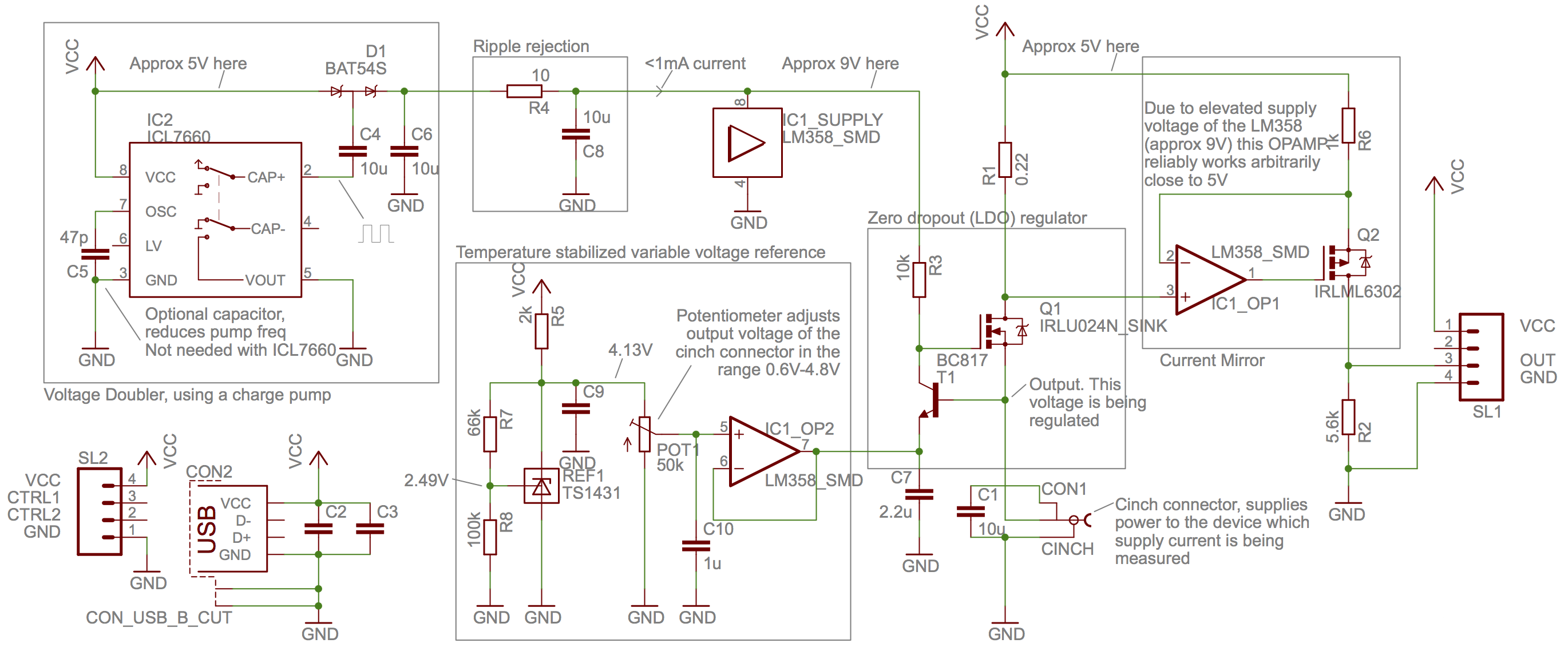
The power board is the only part that makes the complete system a power meter. The rest of the system is just a generic oscilloscope. By replacing the power board, the system can be converted into a different measuring device. In that case, only the power board would need to be replaced with a different board such that it forwards the value of interest towards the converter board.
ADC board
This board has two connections. It accepts an analog signal from the power board, samples it and outputs a digital bit-stream towards the hub board. We use an LTC2314-14, but any device with an SPI interface is compatible. The circuit diagram consists of two main stages, an operational amplifier that ensures a high input impedance and the ADC itself.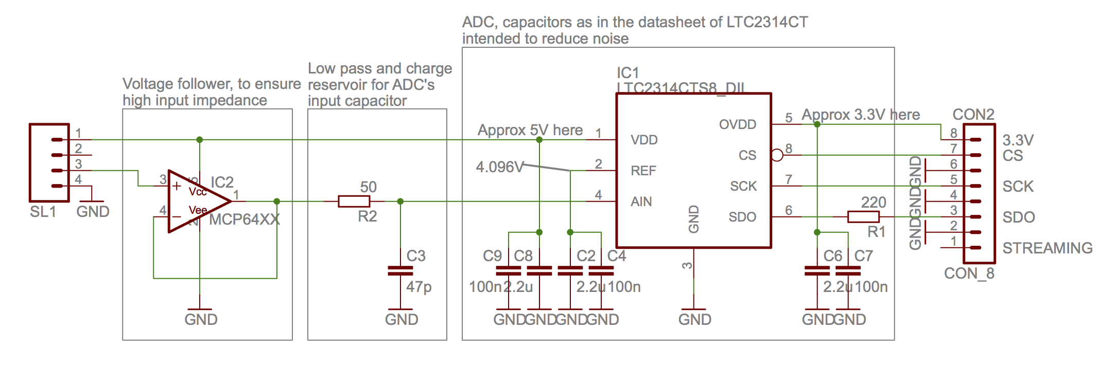
Hub board
This board interfaces with the Raspberry Pi and serves as a generic user interface housing all the LEDs and buttons. It also provides further connectors for the other modules, including the ADC converter board, the power board, and an external connector for the digital channel input.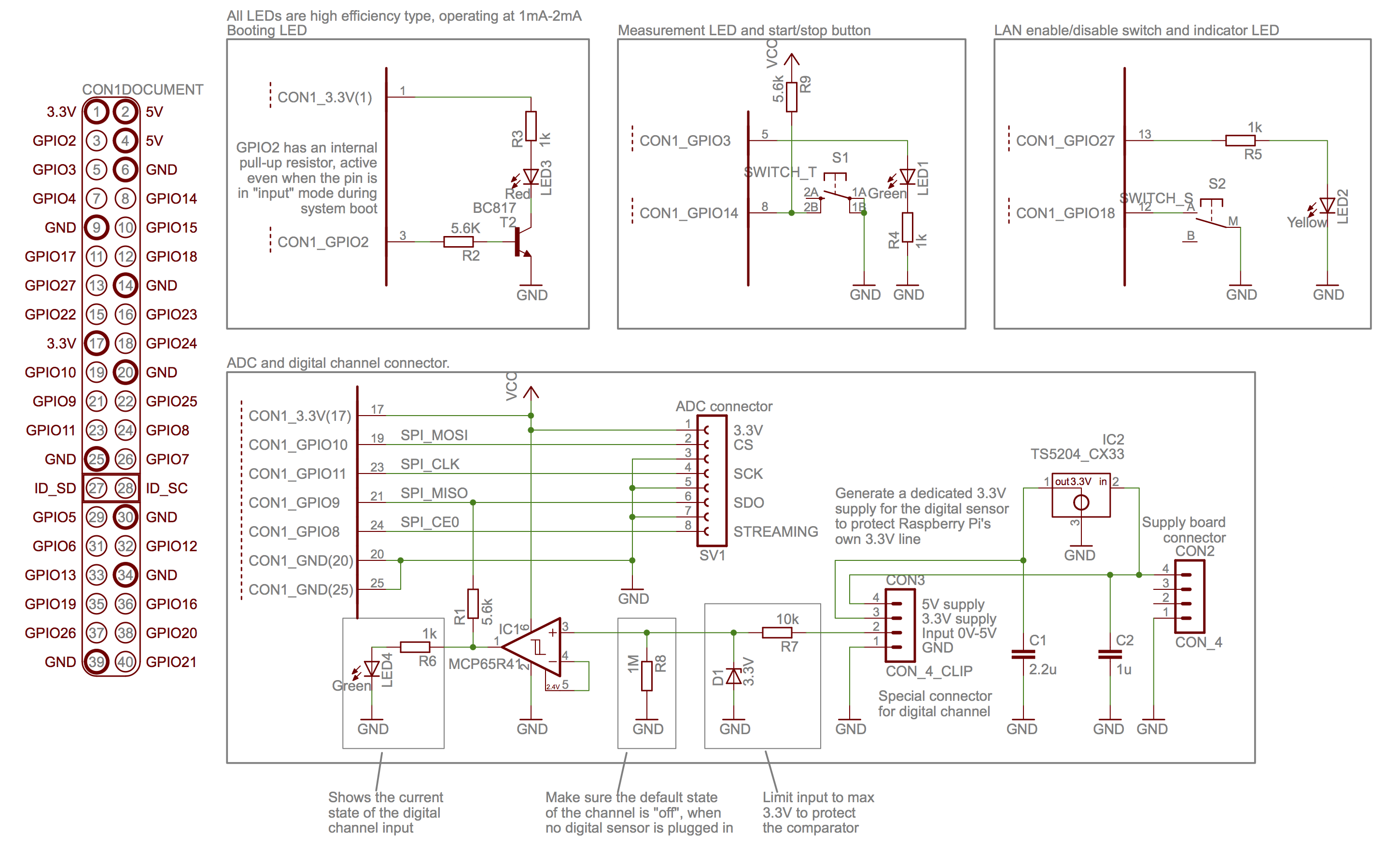
License
The hardware design is licensed under Creative Commons - ShareAlike 3.0 License. More information about the license can be here. A full text version of the license is available here.To got back to the overall overview click here.